
But that monopoly position makes some people, and governments, uneasy. The chipmaking field is essentially controlled by only two big players: ASML, which creates the lithography machines, and TSMC, the chipmaking giant in Taiwan, which uses ASML’s machines to craft the vast majority of all microchips. This duopoly is so powerful that it has geopolitical implications. In an effort to prevent China from developing advanced AI, the US government pressured the Dutch government to impose an embargo in 2019: ASML isn’t allowed to sell high-end machines to any Chinese firm. Geopolitically, “chips are the new oil,” says Marc Hijink, the author of Focus: The ASML Way. Being deprived of them can be as disastrous as being deprived of oil. And in that metaphor, you might say, ASML is the Strait of Hormuz.
James Proud, the cofounder and CEO of the lithography startup Substrate, says the situation is not ideal. The US is “dangerously reliant” on a supply chain that’s overseas and increasingly pricey, Substrate says on its website. “There’s a huge concentration in a small number of players,” Proud says. “And the supply chain is just very expensive.”
Which is why, after two decades of ASML’s dominance, would-be competitors are now gunning for its territory. China is hungrily pouring billions into trying to replicate ASML’s tech. And startups like Substrate are trying to get in the game as well, setting their sights on creating lithography machines that are cheaper, smaller, and even more capable than ASML’s behemoths. Will any of them succeed? The near future clearly belongs to ASML, but as its engineers well know, you can unseat a giant with the right trick of the light.
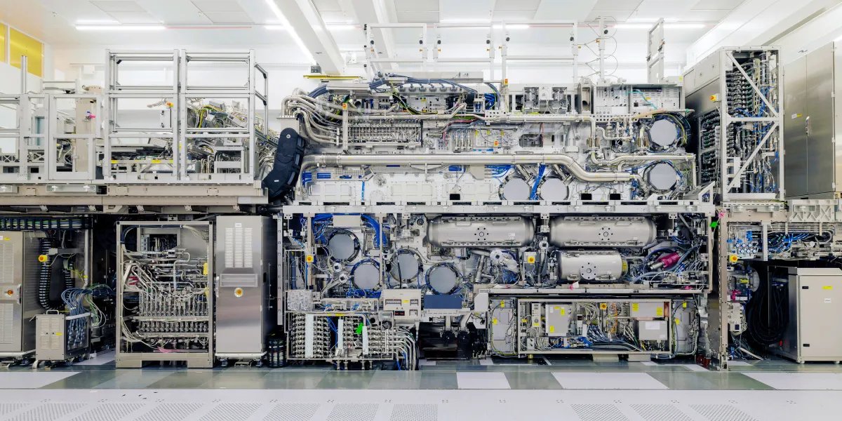
Making chips is, oddly, a bit like silk-screening a T-shirt. To print a pattern on a silicon wafer, you start with a pattern on a reticle—a mask that carries the design. Shining a light on the reticle transfers that pattern to the wafer. The light interacts with a layer of chemicals on the wafer, fixing the pattern in place.
The size of a chip’s features is partly set by the wavelength of light the machine uses: The smaller the wavelength, the teensier the circuitry you can create. You can stretch the capabilities of a wavelength somewhat; increasing what’s known as the numerical aperture, which usually means swapping in a bigger lens, can further focus the light and thus lay down patterns for smaller and smaller components. Eventually, though, this trick hits its limit, and you need to find a new form of light with a smaller wavelength.
So the history of chipmaking has been a two-step dance. The industry finds a good source of light, eventually increases the numerical aperture, and then finally accepts the need for a smaller wavelength, starting the two-step all over again. Up to the early 1990s, chipmakers used visible light, with a wavelength of about 400 nanometers. By the mid-’90s they’d upgraded to deep ultraviolet, ultimately getting it down to a 193-nanometer wavelength. By the late ’90s they saw the end of the line approaching for deep ultraviolet. But what would come next?
All the options were troublesome. They could shift to x-rays, with a teensy one-nanometer wavelength, but they were devilishly hard to focus. Beams of electrons and ions were equally precise; but they worked like dot-matrix printers, transferring a pattern point by point, which was far too slow. (The chip industry wants a machine to crank out hundreds of wafers per hour.)
“It’s a very engineering-heavy company: Let’s send thousands of engineers and just have them mow down these problems. That’s what they did, and it worked.”
Jeff Koch, analyst, SemiAnalysis
Around 2001, ASML, then a smaller player in the lithography world, placed its bet on another option: EUV, with a wavelength just shy of the x-ray range. Nikon and Canon were working on it as well, but they dropped out—while ASML kept going. The idea was full of unknowns. Nobody knew how to reliably generate that type of light, nor how to focus it; EUV is absorbed by regular glass lenses. It’s even absorbed by air. ASML figured it would take six full years to wade through this R&D nightmare.