 dailynewsnblog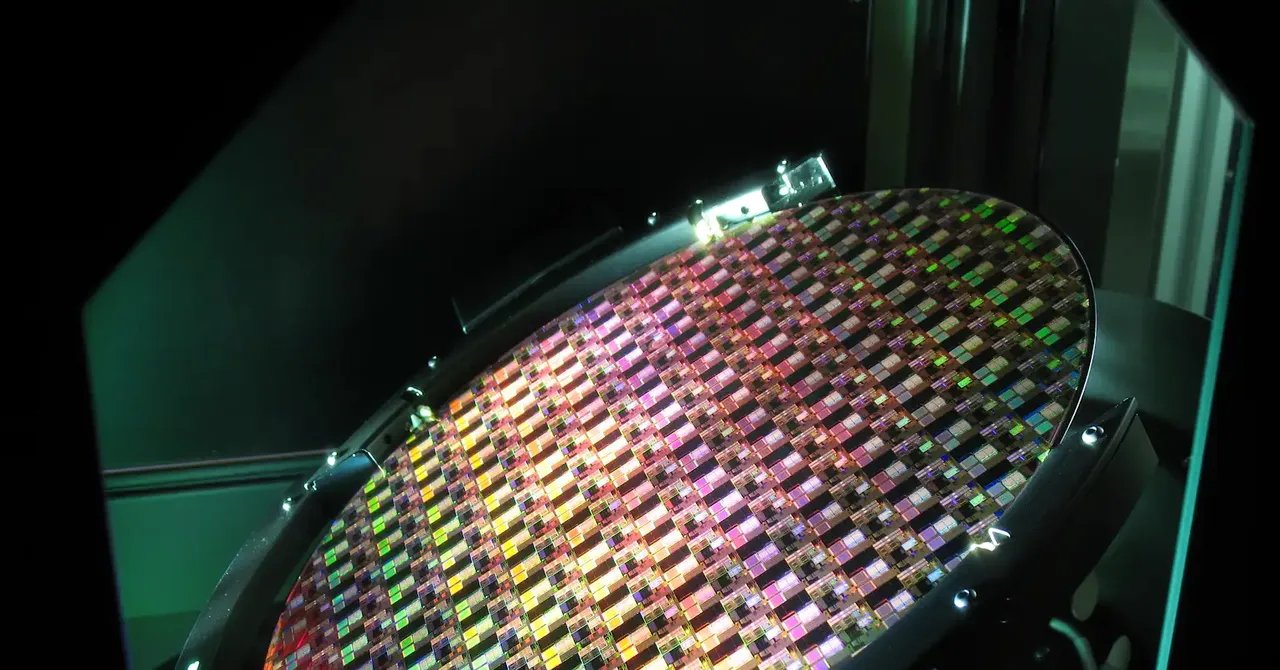
Kepler also says it has improved the density of SRAM using ferroelectrics, which can read and write data at lower voltages than the mechanisms typically used to process and store data in semiconductors. The startup did this by developing a new, low-voltage, composite material that works with this ferroelectric approach.
Sasi Manipatruni, a Kepler cofounder and its chief technology officer, says the Kepler team went through 35 iterations of composites before they landed on a material class that they thought would make memory chips easier and cheaper to make.
“Once we found a way to solve the physics problem—as in the physical limitations for HBM—we came up with a material innovation that helps with the amount of memory you can have between chips,” he says.
In its early build-outs with GlobalFoundries, Kepler says it was able to convert a fab into a “next-generation” fab in just eight months, compared to a typical 24-month timeframe.
“Out goal is to take the fabs and architectures already built, and push them to the limits of physics,” Olaosebikan says.
Basically Kepler is betting that any additional costs that come from new materials or retooling existing fabs would far outweigh the $20 billion to $40 billion it costs to build new ones and outfit them with equipment worth hundreds of millions of dollars.
Waiting to Scale
Kepler Computing still has a long road ahead before it reaches full-scale production—assuming it gets there. To date, the company has run its technology on around 2,000 wafers. The startup says it’s planning to ship its first samples of HBM chips later this year, ramp up production out of Singapore next year, and start chip production in the US in 2028.
Kaste, the GlobalFoundries executive, says he’s confident that the “fundamental breakthroughs have happened. What remains is getting good results on thousands of wafers and millions of devices.”
He points out that one of the challenges with a material system like the one Kepler is using is that it includes iron in its composite. “Iron is a tough contaminant to introduce into a production facility. So Kepler’s solution has to run on dedicated equipment, or be fully encapsulated so that it can’t escape,” he says.
“The art is in keeping that material really well isolated through our production flow,” Kaste says.