

It’s still an extremely challenging proposition. “Packaging is not as easy as saying, ‘I want to run 100,000 wafers per month,’” says Jim McGregor, a longtime chip industry analyst and the founder of Tirias Research, referring to a continuous flow of chips in various stages of production. “It really comes down to whether Intel’s [packaging] fabs can make deals. If we see them expanding those operations more, that’s an indicator that they have.”
Last month, Anwar Ibrahim, the prime minister of Malaysia, revealed in a post on Facebook that Intel is expanding its Malaysian chip-making facilities, which were first established back in the 1970s. Ibrahim said the head of Intel’s Foundry, Naga Chandrasekaran, had “outlined plans to commence the first phase” of expansion, which would include advanced packaging.
“I welcome Intel’s decision to begin operations for the complex later this year,” a translated version of Ibrahim’s post read. An Intel spokesperson, John Hipsher, confirmed that it’s building out additional chip assembly and test capacity in Penang, “amid rising global demand for Intel Foundry packaging solutions.”
Package Store
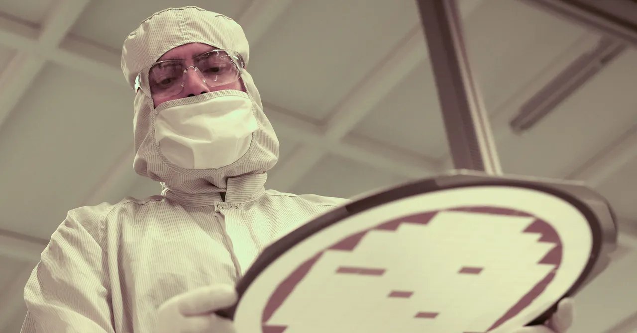
According to Chandrasekaran, who took over Intel’s Foundry operations in 2025 and spoke exclusively with WIRED during the reporting of this story, the term “advanced packaging” itself didn’t exist a decade ago.
Chips have always required some sort of integration of transistors and capacitors, which control and store energy. For a long time the semiconductor industry was focused on miniaturization, or, shrinking the size of components on chips. As the world began demanding more from its computers in the 2010s, chips started to get even more dense with processing units, high-bandwidth memory, and all of the necessary connective parts. Eventually, chipmakers started to take a system-in-packages or package-on-package approach, in which multiple components were stacked on top of one another in order to squeeze more power and memory out of the same surface space. 2D stacking gave way to 3D stacking.
TSMC, the world’s leading semiconductor manufacturer, began offering packaging technologies like CoWoS (chip on wafer on substrate) and, later, SoIC (system on integrated chip) to customers. Essentially, the pitch was that TSMC would handle not just the front end of chip-making—the wafer part—but also the back end, where all of the chip tech would be packaged together.
Intel had ceded its chip manufacturing lead to TSMC at this point, but continued to invest in packaging. In 2017 it introduced a process called EMIB, or embedded multi-die interconnect bridge, which was unique because it shrunk the actual connections, or bridges, between the components in the chip package. In 2019, it introduced Foveros, an advanced die-stacking process. The company’s next packaging advancement was a bigger leap: EMIB-T.
Announced last May, EMIB-T promises to improve power efficiency and signal integrity between all the components on the chips. One former Intel employee with direct knowledge of the company’s packaging efforts tells WIRED that Intel’s EMIB and EMIB-T are designed to be a more “surgical” way of packaging chips than TSMC’s approach. Like most chip advancements, this is supposed to be more power efficient, save space, and, ideally, save customers money in the long runThe company says EMIB-T will roll out in fabs this year.